Flip-flop (electronics)
For the type of shoes (sandals), see Flip-flops

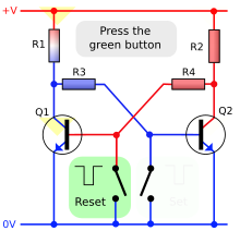
In electronics, a flip-flop or latch is a circuit that has two stable states and can be used to store information. Signals applied to control inputs can change the circuit’s state. It is the basic storage element in sequential logic. Flip-flops and latches are fundamental building blocks of digital electronics systems used in computers, communications, and many other types of systems.
Flip-flops are mainly used as static RAM to store data in a computer. That data is represented in binary. Binary is represented in a 1 (“high state”) and 0 (“low state”). The structure of flip flops vary, but the general characteristic is that two branches affect each other's state by putting the current resulting state of one branch and using that as input for the next iteration of the other branch.

History
changeThe first electronic flip-flop, originally called the Eccles-Jordan trigger circuit, was invented in 1918 by the British physicists William Eccles and F. W. Jordan.[1][2] The initial design’s only active elements were two vacuum tubes.[3] While working at Hughes Aircraft, Eldred Nelson coined the term JK for a flip-flop which changed states when both inputs were on (a logical "one").
Implementation
changeFlip-flops can be either simple or clocked. A simple flip-flop changes state as soon as the input changes. A clocked flip-flop changes state only when an extra pulse occurs. This pulse is called the clock signal. Commonly, flip-flop only refers to clocked circuits; the simple ones are commonly called latches.
Types
changeThe two common types of flip-flops are SR ("set-reset"), D ("data" or "delay").
SR flip-flop
changeThe most fundamental flip-flop is the simple SR flip-flop. In the SR flip-flop, the S and R stand for set and reset. The stored bit is present on the output marked Q.
If S is pulsed high while R is held low, then the Q output is forced high. Conversely, if R is pulsed high while S is held low, then the Q output is forced low. When the R and S inputs are both low, the Q outputs are in a constant state. However, when the R and S inputs are both high, the Q outputs are in a forbidden state.
Since high and low mean logical '1' and '0', respectively, the SR flip-flop can have four combinations showing below:
(A) S = 1, R = 0: set
(B) S = 0, R = 0: hold
(C) S = 0, R = 1: reset
(D) S = 1, R = 1: not allowed
The restricted combination (D) leads to an unstable state.
D Flip-flop
changeA D Flip-Flop prevents an SR flip-flop from receiving the forbidden combination. It takes only one input for data, called D. It splits this data down two paths. On one path it flips the data to the opposite value. This is the “NOT” box in the animation. That way, S = 1, R = 1 is never fed to the internal SR latch.
References
change- ↑ William Henry Eccles and Frank Wilfred Jordan, "Improvements in ionic relays Archived 2008-10-12 at the Wayback Machine" British patent number: GB 148582 (filed: 21 June 1918; published: 5 August 1920).
- ↑ See:
- W. H. Eccles and F. W. Jordan (19 September 1919) "A trigger relay utilizing three-electrode thermionic vacuum tubes," The Electrician, 83 : 298.
- Reprinted in: W. H. Eccles and F. W. Jordan (December 1919) "A trigger relay utilizing three-electrode thermionic vacuum tubes," The Radio Review, 1 (3) : 143–146.
- Summary in: W. H. Eccles and F. W. Jordan (1919) "A trigger relay utilising three electrode thermionic vacuum tubes," Report of the Eighty-seventh Meeting of the British Association for the Advancement of Science: Bournemouth: 1919, September 9–13, pp. 271–272.
- ↑ Pugh, Emerson W.; Johnson, Lyle R.; Palmer, John H. (1991). IBM's 360 and early 370 systems. MIT Press. p. 10. ISBN 978-0-262-16123-7.